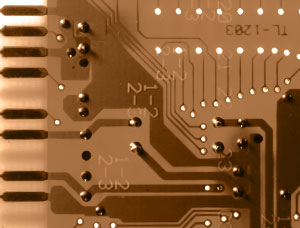
Topography protection is intended for microelectronic semiconductor products.
Its practical significance is small as patent protection is usually applied for in its place.
Topography protection is intended for microelectronic semiconductor products.
Its practical significance is small as patent protection is usually applied for in its place.